I’ve spent my last week and a half’s free time going back and forth among EAGLE, eagle3d, 1:1 printouts, and the Viewplot Gerber viewer. That’s how long it took me to get the silkscreen layer tweaked to my satisfaction — which I completely didn’t anticipate.
Thank you, thank you, thank you SparkFun for emphasizing how important it is to view your Gerbers before submitting (search in page for “Something I highly recommend”).
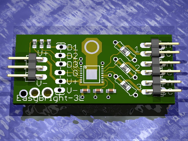
I had already rendered the board layout in eagle3d (pay no mind to the test holes I used to figure out that eagle3d doesn’t make holes through copper that’s part of a polygon, which its documentation clearly states if you bother to read it) and thought it looked pretty good.
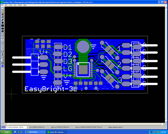
But I followed Nate’s advice, installed Viewplot, and was rather startled to see what my board was really going to look like.
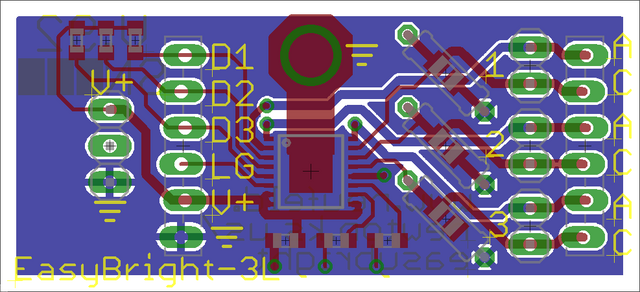
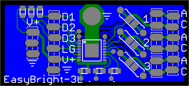
The silkscreened boxes for the plastic “keepers” on the pin headers are fairly faithful to the connectors I’m using, but what’s with putting the pins in the silkscreen? I don’t need a shadow of the pins on the board.
Also the 0805 SMT resistors and capacitors don’t have silk around them showing which pads belong to the same component. It’s easy enough to figure out on this small board, but I’d like to develop good habits.
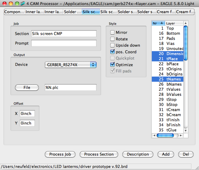
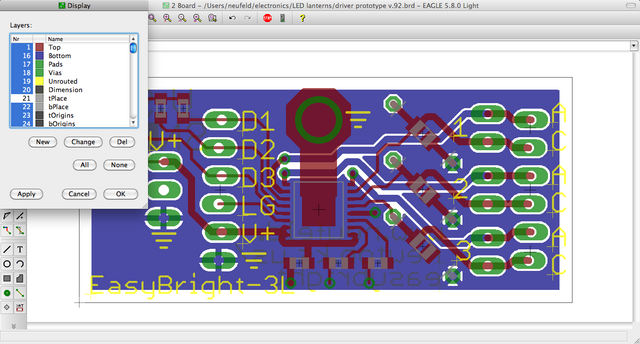
EAGLE’s CAM processor lets you pick which PCB layers are used to generate each Gerber file, and there’s not much in my top silk layer. The pins must be in tPlace, so I used the PCB layout editor to preview what would happen if I turned it off …
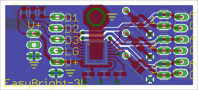
I lost the header outlines as well as the pins, as well as the outlines for the optional through-hole resistors. That’s not gonna work.
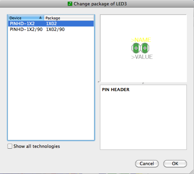
Exercising outrageous optimism, I tried changing my header packages from right-angle to vertical, hoping they’d have more appropriate package outlines (still in the tPlace layer).
Better — no stray pins in the silkscreen. Now guardedly optimistic.
I turned off the tDocu layer that shows the physical outlines of components, and which isn’t (and mustn’t be) included in the silkscreen Gerber because it would interfere with soldering, then added lines in tPlace to indicate the edges of SMT components.
Silly me — I thought I was done!
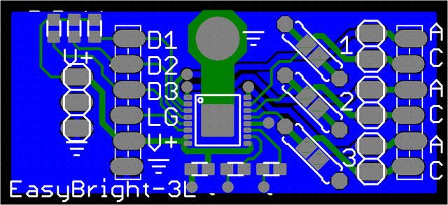
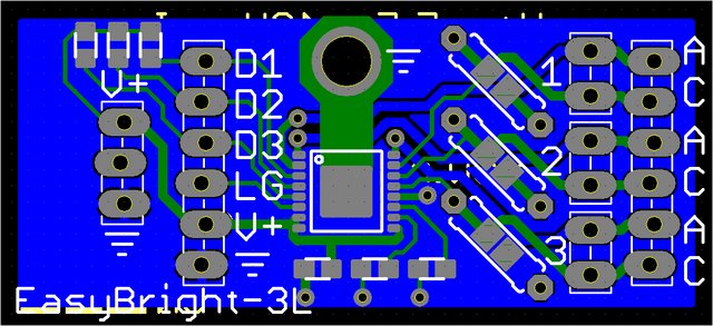
Back in Viewplot, look at how the silkscreen around the power connector is now crowding the pin labels. Aaargh! There’s not room to move them far enough away.
I went back to my connector library and designed two- and three-pin versions of “locking” connectors based on the SparkFun locking connector concept. (See footnote about SparkFun EAGLE library license terms.)
The Gerber view looked pretty good now, except the ground symbol was too close to the power header and a little visually confusing.
I moved that down a bit and in my next trip to Viewplot discovered how to get the drill holes to show up: don’t load the drill rack file into Viewplot, just the drill file itself. Getting visualization with holes and confirmation that there’s really a mounting hole through the heatsink — outstanding!
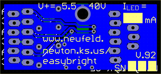
Somewhere around this time I also printed out the solder-side of the board to make sure that the boxes I made to write in (visible in the next screen shot) were large enough for me to write in. They weren’t. I enlarged them.
Done now, maybe?
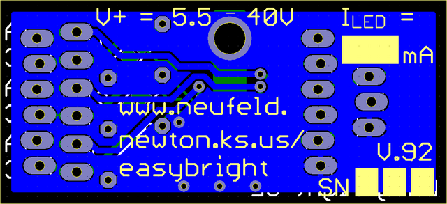
Oof, look at all the problems with the silkscreen on the back side. The top line looks like I’m incrementing V by 5.5-40V (C joke), and if I fix that I need to move ILED‘s = further away also. The / in the URL is awfully close to the solder pad, and the box for me to write the “factory”-configured LED current could stand to extend a little closer to the “mA” label.
Props to Nate at SparkFun again (search in page for “Label everything, all the time”) for reminding me to put the input voltage range and output current rating on the board, BTW.
Fixed! Really! Done! If I stare at this thing any longer, I’m going to start hand-kerning the vector font.
I zipped the files and uploaded them to Gold Phoenix last night.
SparkFun EAGLE Library License Terms
I’m not using SparkFun’s EAGLE library nor a derivative of their library file because I haven’t got a response from them whether their cc-by-sa license is intended to be:
- like the GPL, meaning that if you use their library in your board design you have to open-source your whole design — which I will do after I’m confident the design is right but not immediately upon shipping — or
- like the LGPL and you can use the library in your product without open-sourcing your design but you would have to open-source derivatives of the library itself.
So my connector library is most definitely based on Pete Lewis’s idea to skew pin positioning from side to side to make a header friction-fit in a board for soldering, but (as far as I know) the idea is not patented and I’m in the clear. My library is a reimplementation from scratch of the idea, so is not derivative of their library.
I hate playing games like this and I would love to toss my library and use SparkFun’s if I can get a verdict from them on the licensing. Also as soon as I’ve got boards tested and working and I’m ready to publish the design files, I can switch back to their library too.
Update 07-May-2010: I heard back from SparkFun and it will be fine for me to use their library. I’ll look at switching back on the next iteration of the board.
Ah.
You do have a bit of a bug on your boards; I hope you didn’t submit them to manufacturing yet.
The third SMD current sense resistor is not properly connected to its TH version – one of the legs is floating.
AAARGH.
And the bug exists on my schematic as well, which I know it didn’t used to. Probably introduced it when I was rotating the SMT resistors to make their values read in the “right” orientation in eagle3d. That’ll teach me!
I have submitted the boards already and I’ve now emailed them to ask whether I’m too late to change. Thank you!
Thanks for the catch!
I use gerbv to review my gerbers – it always pays to double (and triple) check everything!
Regarding Sparkfun’s libraries, I have found that while their libraries are helpful, they are rarely exactly what I want. So I stopped using them. Not only was I worried about their license terms, but it is faster and easier for me to draft my own footprints and symbols in Eagle than try to modify their existing ones.
I think if you do a survey of Eagle users, most serious users are creating their own footprints for all but the most common components. That way you get to set up all of the layers just the way you want! Most of the component libraries (especially surface mount parts) that ship with Eagle are pretty terrible anyway!
Jeff, gerbv looks like a good option; thanks! I’d much rather go back and forth between my MacBook and my Linux workstation (which Unison-syncs with the MacBook) than my MacBook and a Windows machine (at the office).
I’ve had some grief with the Sparkfun “lock-in” headers. First, the center of the part is not in the center but is on one end. If you rotate the part, the position moves wildly.
A potentially bigger problem is with the keyed single row headers. Sparkfun’s pin numbers are opposite of those by Molex (and presumably most other people). I almost put my PIC ICSP connectors in backwards before I discovered this “difference.”
Jon