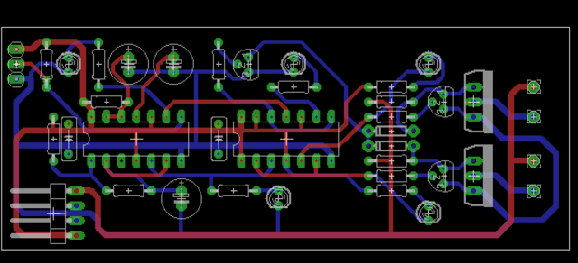
I’m working on a PC board layout for a circuit I’ve built and tested on the workbench. I enjoy board layout, but I was still delighted to be finished with the design. I printed out a copy, not to test whether all the components fit, but to stare at for a day and see whether I found anything that might need to be corrected.
Boy, did I.
In general, the first stage of laying out a PCB is placing external interface components — connectors, switches, potentiometers, etc. — followed closely by other large components and power supply traces. For me, the last stage of layout is doing a sanity check that the board will actually work (and be possible to assemble) in the real world.
Here’s what I found.
